欢迎光临~泰州巨纳新能源有限公司
语言选择:
 ∷
∷

∷
 ∷
∷

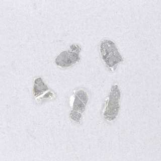


六方氮化硼晶体(20片装) hBN(Hexagonal Boron Nitride)-Crystal
晶体尺寸:~1mm
电学性能:绝缘体/半导体
晶体结构:六边形
晶胞参数:a = b = 0.2502 nm, c = 0.6617 nm, α = β = 90°, γ = 120°
晶体类型:合成
晶体纯度:A级
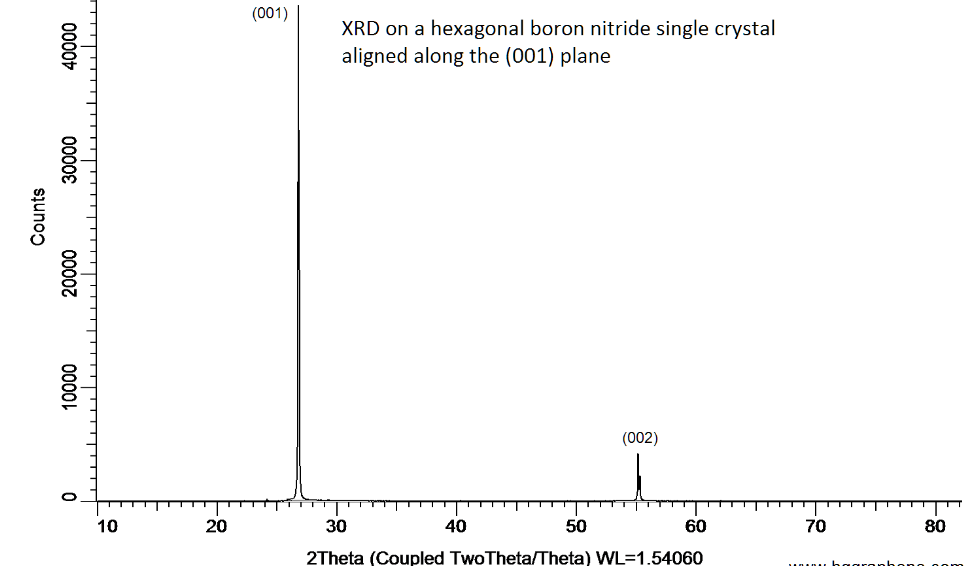
X-ray diffraction on a hexagonal boron nitride single crystal aligned along the (001) plane. XRD was performed at room temperature using a D8 Venture Bruker. The 4 XRD peaks correspond, from left to right, to (00l) with l = 1, 2, 3

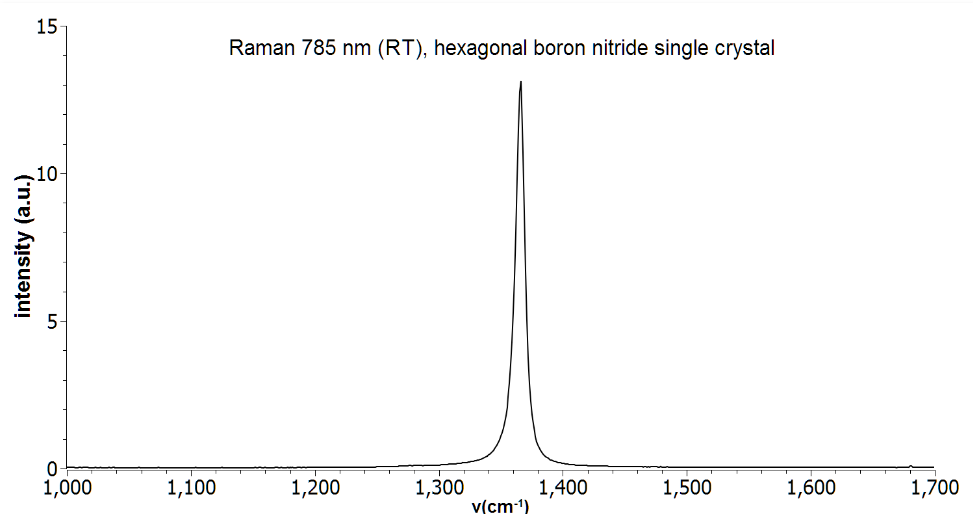
Raman spectrum of a single crystal hexagonal boron nitride (h-BN). Measurement was performed with a 785nm Raman system at room temperature.
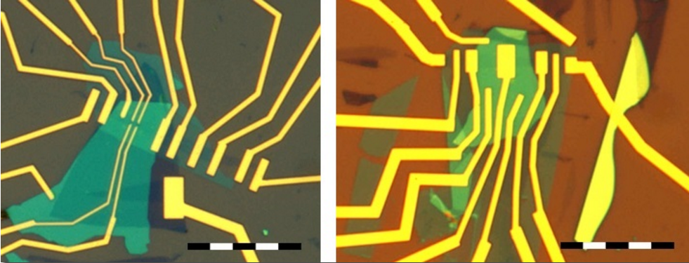
Device at left side: Fabrication of a high mobiltity bilayer graphene. This field effect transistor is fabricated using the polymer 2D_CL_PC ( click here ). The device is composed out of four 2D layers. The bilayer graphene is encapsulated between two hexagonal boron nitride crystals (h-BN). The fourth layer is a thin layer of graphite (HOPG) which is used as a backgate. Scale bar is 20μm. Device at right side: This device is similar to the one at the left side, here we added on the top hexagonal boron nitride layer a gold electrode in order to apply a top gate voltage to the hBN encapsulated bilayer graphene. Scale bar is 20μm
联系人:严春伟
手机:13914543285
电话:0523-86190619,86192878
邮箱:taizhou@sunano.com.cn
地址: 江苏省泰州市凤凰西路168号