欢迎光临~泰州巨纳新能源有限公司
语言选择:
 ∷
∷

∷
 ∷
∷
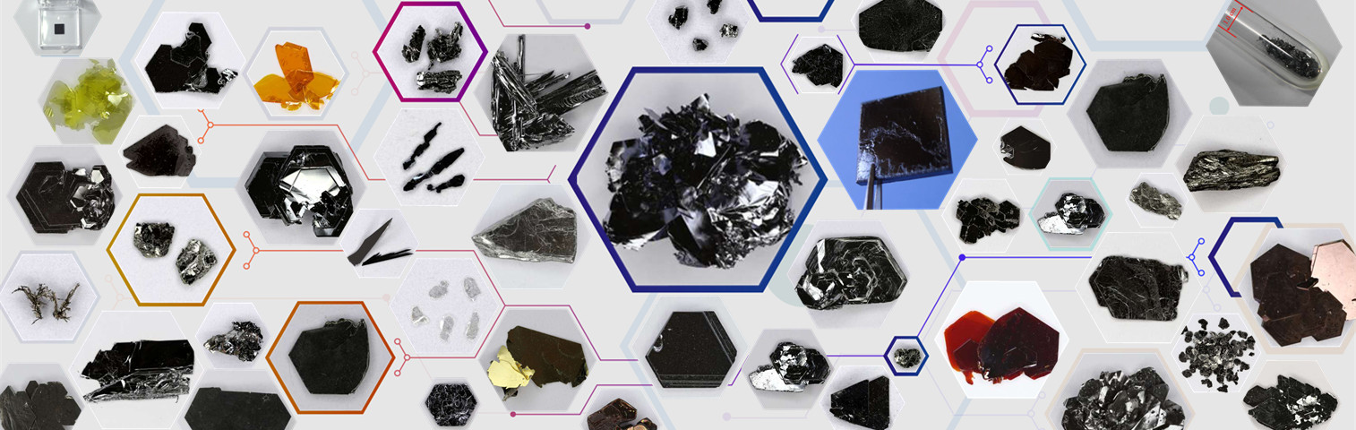

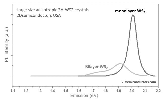
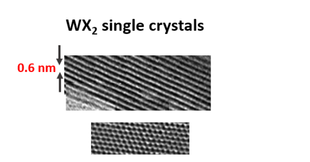
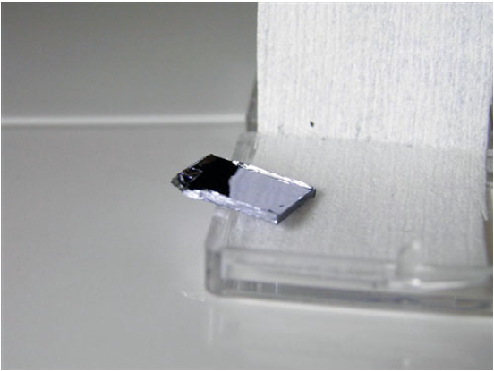
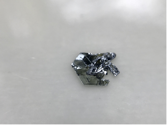
More than a decade of growth optimization in chemical vapor transport (CVT) as well as flux growth lead to our flawless WS2 crystals. Our p-type WS2 crystals are doped with Nb atoms at 1E17-5E18cm-3 range. These electronically doped vdW WS2 crystals are treated as gold standards in 2D materials field. WS2 crystals from 2Dsemiconductors are known for its superior valleytronic performance, perfect crystallization, defect free structure, extremely narrow PL bandwidths, clean PL spectra (free of bound exciton shoulders), and high carrier mobility. Thousands of scientific articles have cited us and used these crystals for scientific accuracy and clean signals. Please also see our n- and p-type WS2 crystals doped with Au, Re, Nb, or other transition metal atoms.
Please note that doping into TMDCs greatly reduce the crystallization time (growth speeds), thus electronically doped TMDCs measure smaller than undoped (intrinsic) TMDCs.
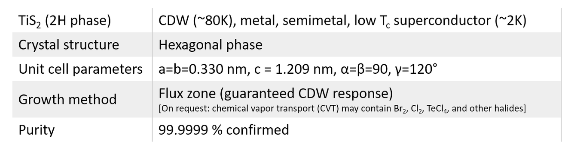
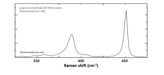
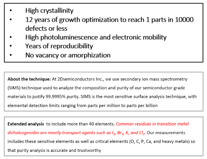
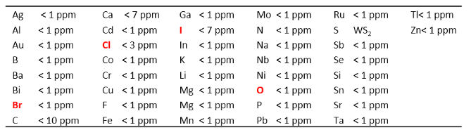
Typical characteristics of WS2 crystals from 2Dsemiconductors
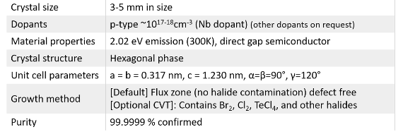
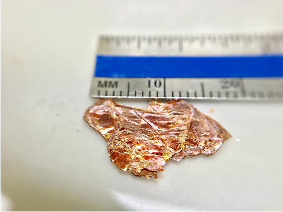
Growth method matters> Flux zone or CVT growth method? Contamination of halides and point defects in layered crystals are well known cause for their reduced electronic mobility, reduced anisotropic response, poor e-h recombination, low-PL emission, and lower optical absorption. Flux zone technique is a halide free technique used for synthesizing truly semiconductor grade vdW crystals. This method distinguishes itself from chemical vapor transport (CVT) technique in the following regard: CVT is a quick (~2 weeks) growth method but exhibits poor crystalline quality and the defect concentration reaches to 1E11 to 1E12 cm-2 range. In contrast, flux method takes long (~3 months) growth time, but ensures slow crystallization for perfect atomic structuring, and impurity free crystal growth with defect concentration as low as 1E9 - 1E10 cm-2. During check out just state which type of growth process is preferred. Unless otherwise stated, 2Dsemiconductors ships Flux zone crystals as a default choice.
http://meetings.aps.org/Meeting/MAR18/Session/K36.3
http://meetings.aps.org/Meeting/MAR17/Session/V1.14


联系人:严春伟
手机:13914543285
电话:0523-86190619,86192878
邮箱:taizhou@sunano.com.cn
地址: 江苏省泰州市凤凰西路168号